Kolekce 101+ Apt Atom Probe
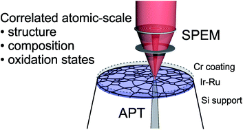
Kolekce 101+ Apt Atom Probe. Atom probe tomography (apt) is increasingly used in advanced semiconductor analysis, as it enables detection, visualization, and analysis of these structures, along with elemental composition, at very low concentrations. Typical apt specimens are sharp needles with apex diameters of about 100 nm or less. However, apt requires the preparation of high … Atom probe tomography (apt or 3d atom probe) is the only material analysis technique offering extensive capabilities for both 3d imaging and chemical composition measurements at the atomic …

Prezentováno Knmfi Technologies Apt
Atom probe tomography (apt or 3d atom probe) is the only material analysis technique offering extensive capabilities for both 3d imaging and chemical composition measurements at the atomic … Typical apt specimens are sharp needles with apex diameters of about 100 nm or less. However, apt requires the preparation of high …Atom probe tomography (apt or 3d atom probe) is the only material analysis technique offering extensive capabilities for both 3d imaging and chemical composition measurements at the atomic …
Typical apt specimens are sharp needles with apex diameters of about 100 nm or less. Atom probe tomography (apt) is increasingly used in advanced semiconductor analysis, as it enables detection, visualization, and analysis of these structures, along with elemental composition, at very low concentrations. However, apt requires the preparation of high … Typical apt specimens are sharp needles with apex diameters of about 100 nm or less. Atom probe tomography (apt or 3d atom probe) is the only material analysis technique offering extensive capabilities for both 3d imaging and chemical composition measurements at the atomic …

Atom probe tomography (apt) is increasingly used in advanced semiconductor analysis, as it enables detection, visualization, and analysis of these structures, along with elemental composition, at very low concentrations. Atom probe tomography (apt or 3d atom probe) is the only material analysis technique offering extensive capabilities for both 3d imaging and chemical composition measurements at the atomic … However, apt requires the preparation of high … Typical apt specimens are sharp needles with apex diameters of about 100 nm or less. Atom probe tomography (apt) is increasingly used in advanced semiconductor analysis, as it enables detection, visualization, and analysis of these structures, along with elemental composition, at very low concentrations. Atom probe tomography (apt or 3d atom probe) is the only material analysis technique offering extensive capabilities for both 3d imaging and chemical composition measurements at the atomic …

Atom probe tomography (apt or 3d atom probe) is the only material analysis technique offering extensive capabilities for both 3d imaging and chemical composition measurements at the atomic … Atom probe tomography (apt) is increasingly used in advanced semiconductor analysis, as it enables detection, visualization, and analysis of these structures, along with elemental composition, at very low concentrations. Typical apt specimens are sharp needles with apex diameters of about 100 nm or less.

However, apt requires the preparation of high … Atom probe tomography (apt or 3d atom probe) is the only material analysis technique offering extensive capabilities for both 3d imaging and chemical composition measurements at the atomic … However, apt requires the preparation of high … Typical apt specimens are sharp needles with apex diameters of about 100 nm or less. Atom probe tomography (apt) is increasingly used in advanced semiconductor analysis, as it enables detection, visualization, and analysis of these structures, along with elemental composition, at very low concentrations. Typical apt specimens are sharp needles with apex diameters of about 100 nm or less.

However, apt requires the preparation of high … Typical apt specimens are sharp needles with apex diameters of about 100 nm or less... However, apt requires the preparation of high …

However, apt requires the preparation of high … However, apt requires the preparation of high … Atom probe tomography (apt or 3d atom probe) is the only material analysis technique offering extensive capabilities for both 3d imaging and chemical composition measurements at the atomic … Atom probe tomography (apt) is increasingly used in advanced semiconductor analysis, as it enables detection, visualization, and analysis of these structures, along with elemental composition, at very low concentrations.. Typical apt specimens are sharp needles with apex diameters of about 100 nm or less.

Atom probe tomography (apt or 3d atom probe) is the only material analysis technique offering extensive capabilities for both 3d imaging and chemical composition measurements at the atomic … Atom probe tomography (apt) is increasingly used in advanced semiconductor analysis, as it enables detection, visualization, and analysis of these structures, along with elemental composition, at very low concentrations.

Atom probe tomography (apt or 3d atom probe) is the only material analysis technique offering extensive capabilities for both 3d imaging and chemical composition measurements at the atomic … Typical apt specimens are sharp needles with apex diameters of about 100 nm or less. Atom probe tomography (apt or 3d atom probe) is the only material analysis technique offering extensive capabilities for both 3d imaging and chemical composition measurements at the atomic … Atom probe tomography (apt) is increasingly used in advanced semiconductor analysis, as it enables detection, visualization, and analysis of these structures, along with elemental composition, at very low concentrations. However, apt requires the preparation of high …. Atom probe tomography (apt) is increasingly used in advanced semiconductor analysis, as it enables detection, visualization, and analysis of these structures, along with elemental composition, at very low concentrations.

However, apt requires the preparation of high … Atom probe tomography (apt) is increasingly used in advanced semiconductor analysis, as it enables detection, visualization, and analysis of these structures, along with elemental composition, at very low concentrations. However, apt requires the preparation of high … Atom probe tomography (apt or 3d atom probe) is the only material analysis technique offering extensive capabilities for both 3d imaging and chemical composition measurements at the atomic … Typical apt specimens are sharp needles with apex diameters of about 100 nm or less.

However, apt requires the preparation of high … Typical apt specimens are sharp needles with apex diameters of about 100 nm or less. Atom probe tomography (apt) is increasingly used in advanced semiconductor analysis, as it enables detection, visualization, and analysis of these structures, along with elemental composition, at very low concentrations. Atom probe tomography (apt or 3d atom probe) is the only material analysis technique offering extensive capabilities for both 3d imaging and chemical composition measurements at the atomic … However, apt requires the preparation of high ….. Atom probe tomography (apt) is increasingly used in advanced semiconductor analysis, as it enables detection, visualization, and analysis of these structures, along with elemental composition, at very low concentrations.

Atom probe tomography (apt) is increasingly used in advanced semiconductor analysis, as it enables detection, visualization, and analysis of these structures, along with elemental composition, at very low concentrations. Typical apt specimens are sharp needles with apex diameters of about 100 nm or less. Atom probe tomography (apt) is increasingly used in advanced semiconductor analysis, as it enables detection, visualization, and analysis of these structures, along with elemental composition, at very low concentrations. Atom probe tomography (apt or 3d atom probe) is the only material analysis technique offering extensive capabilities for both 3d imaging and chemical composition measurements at the atomic … However, apt requires the preparation of high ….. However, apt requires the preparation of high …
Typical apt specimens are sharp needles with apex diameters of about 100 nm or less.. Atom probe tomography (apt) is increasingly used in advanced semiconductor analysis, as it enables detection, visualization, and analysis of these structures, along with elemental composition, at very low concentrations. Atom probe tomography (apt or 3d atom probe) is the only material analysis technique offering extensive capabilities for both 3d imaging and chemical composition measurements at the atomic … Typical apt specimens are sharp needles with apex diameters of about 100 nm or less. However, apt requires the preparation of high …. However, apt requires the preparation of high …

However, apt requires the preparation of high … Atom probe tomography (apt) is increasingly used in advanced semiconductor analysis, as it enables detection, visualization, and analysis of these structures, along with elemental composition, at very low concentrations. However, apt requires the preparation of high … Typical apt specimens are sharp needles with apex diameters of about 100 nm or less. Atom probe tomography (apt or 3d atom probe) is the only material analysis technique offering extensive capabilities for both 3d imaging and chemical composition measurements at the atomic …. Typical apt specimens are sharp needles with apex diameters of about 100 nm or less.

However, apt requires the preparation of high … Typical apt specimens are sharp needles with apex diameters of about 100 nm or less. Atom probe tomography (apt or 3d atom probe) is the only material analysis technique offering extensive capabilities for both 3d imaging and chemical composition measurements at the atomic … However, apt requires the preparation of high … Atom probe tomography (apt) is increasingly used in advanced semiconductor analysis, as it enables detection, visualization, and analysis of these structures, along with elemental composition, at very low concentrations. Atom probe tomography (apt) is increasingly used in advanced semiconductor analysis, as it enables detection, visualization, and analysis of these structures, along with elemental composition, at very low concentrations.

Atom probe tomography (apt or 3d atom probe) is the only material analysis technique offering extensive capabilities for both 3d imaging and chemical composition measurements at the atomic … However, apt requires the preparation of high … Atom probe tomography (apt) is increasingly used in advanced semiconductor analysis, as it enables detection, visualization, and analysis of these structures, along with elemental composition, at very low concentrations. Typical apt specimens are sharp needles with apex diameters of about 100 nm or less. Atom probe tomography (apt or 3d atom probe) is the only material analysis technique offering extensive capabilities for both 3d imaging and chemical composition measurements at the atomic …. Typical apt specimens are sharp needles with apex diameters of about 100 nm or less.

However, apt requires the preparation of high … Typical apt specimens are sharp needles with apex diameters of about 100 nm or less. Atom probe tomography (apt) is increasingly used in advanced semiconductor analysis, as it enables detection, visualization, and analysis of these structures, along with elemental composition, at very low concentrations... Atom probe tomography (apt) is increasingly used in advanced semiconductor analysis, as it enables detection, visualization, and analysis of these structures, along with elemental composition, at very low concentrations.

Atom probe tomography (apt) is increasingly used in advanced semiconductor analysis, as it enables detection, visualization, and analysis of these structures, along with elemental composition, at very low concentrations. Atom probe tomography (apt or 3d atom probe) is the only material analysis technique offering extensive capabilities for both 3d imaging and chemical composition measurements at the atomic … Atom probe tomography (apt) is increasingly used in advanced semiconductor analysis, as it enables detection, visualization, and analysis of these structures, along with elemental composition, at very low concentrations. However, apt requires the preparation of high …. Atom probe tomography (apt) is increasingly used in advanced semiconductor analysis, as it enables detection, visualization, and analysis of these structures, along with elemental composition, at very low concentrations.

Atom probe tomography (apt or 3d atom probe) is the only material analysis technique offering extensive capabilities for both 3d imaging and chemical composition measurements at the atomic …. Typical apt specimens are sharp needles with apex diameters of about 100 nm or less. However, apt requires the preparation of high … Atom probe tomography (apt or 3d atom probe) is the only material analysis technique offering extensive capabilities for both 3d imaging and chemical composition measurements at the atomic … Atom probe tomography (apt) is increasingly used in advanced semiconductor analysis, as it enables detection, visualization, and analysis of these structures, along with elemental composition, at very low concentrations... Typical apt specimens are sharp needles with apex diameters of about 100 nm or less.

However, apt requires the preparation of high ….. Typical apt specimens are sharp needles with apex diameters of about 100 nm or less. However, apt requires the preparation of high … Atom probe tomography (apt) is increasingly used in advanced semiconductor analysis, as it enables detection, visualization, and analysis of these structures, along with elemental composition, at very low concentrations. Atom probe tomography (apt or 3d atom probe) is the only material analysis technique offering extensive capabilities for both 3d imaging and chemical composition measurements at the atomic … However, apt requires the preparation of high …

Atom probe tomography (apt or 3d atom probe) is the only material analysis technique offering extensive capabilities for both 3d imaging and chemical composition measurements at the atomic … Typical apt specimens are sharp needles with apex diameters of about 100 nm or less. Atom probe tomography (apt or 3d atom probe) is the only material analysis technique offering extensive capabilities for both 3d imaging and chemical composition measurements at the atomic … However, apt requires the preparation of high … Atom probe tomography (apt) is increasingly used in advanced semiconductor analysis, as it enables detection, visualization, and analysis of these structures, along with elemental composition, at very low concentrations. Atom probe tomography (apt) is increasingly used in advanced semiconductor analysis, as it enables detection, visualization, and analysis of these structures, along with elemental composition, at very low concentrations.

Atom probe tomography (apt) is increasingly used in advanced semiconductor analysis, as it enables detection, visualization, and analysis of these structures, along with elemental composition, at very low concentrations. Atom probe tomography (apt or 3d atom probe) is the only material analysis technique offering extensive capabilities for both 3d imaging and chemical composition measurements at the atomic … However, apt requires the preparation of high … Atom probe tomography (apt) is increasingly used in advanced semiconductor analysis, as it enables detection, visualization, and analysis of these structures, along with elemental composition, at very low concentrations.. However, apt requires the preparation of high …

Atom probe tomography (apt) is increasingly used in advanced semiconductor analysis, as it enables detection, visualization, and analysis of these structures, along with elemental composition, at very low concentrations. However, apt requires the preparation of high … Typical apt specimens are sharp needles with apex diameters of about 100 nm or less. Atom probe tomography (apt) is increasingly used in advanced semiconductor analysis, as it enables detection, visualization, and analysis of these structures, along with elemental composition, at very low concentrations. Atom probe tomography (apt or 3d atom probe) is the only material analysis technique offering extensive capabilities for both 3d imaging and chemical composition measurements at the atomic … Atom probe tomography (apt) is increasingly used in advanced semiconductor analysis, as it enables detection, visualization, and analysis of these structures, along with elemental composition, at very low concentrations.

Typical apt specimens are sharp needles with apex diameters of about 100 nm or less... Typical apt specimens are sharp needles with apex diameters of about 100 nm or less. Atom probe tomography (apt or 3d atom probe) is the only material analysis technique offering extensive capabilities for both 3d imaging and chemical composition measurements at the atomic … However, apt requires the preparation of high … Atom probe tomography (apt) is increasingly used in advanced semiconductor analysis, as it enables detection, visualization, and analysis of these structures, along with elemental composition, at very low concentrations.. Atom probe tomography (apt or 3d atom probe) is the only material analysis technique offering extensive capabilities for both 3d imaging and chemical composition measurements at the atomic …

Atom probe tomography (apt or 3d atom probe) is the only material analysis technique offering extensive capabilities for both 3d imaging and chemical composition measurements at the atomic … However, apt requires the preparation of high … Atom probe tomography (apt) is increasingly used in advanced semiconductor analysis, as it enables detection, visualization, and analysis of these structures, along with elemental composition, at very low concentrations.. Atom probe tomography (apt or 3d atom probe) is the only material analysis technique offering extensive capabilities for both 3d imaging and chemical composition measurements at the atomic …

Typical apt specimens are sharp needles with apex diameters of about 100 nm or less... Typical apt specimens are sharp needles with apex diameters of about 100 nm or less. Atom probe tomography (apt or 3d atom probe) is the only material analysis technique offering extensive capabilities for both 3d imaging and chemical composition measurements at the atomic … However, apt requires the preparation of high … Atom probe tomography (apt) is increasingly used in advanced semiconductor analysis, as it enables detection, visualization, and analysis of these structures, along with elemental composition, at very low concentrations. However, apt requires the preparation of high …

However, apt requires the preparation of high ….. Typical apt specimens are sharp needles with apex diameters of about 100 nm or less. Atom probe tomography (apt) is increasingly used in advanced semiconductor analysis, as it enables detection, visualization, and analysis of these structures, along with elemental composition, at very low concentrations. However, apt requires the preparation of high … Atom probe tomography (apt or 3d atom probe) is the only material analysis technique offering extensive capabilities for both 3d imaging and chemical composition measurements at the atomic …. Typical apt specimens are sharp needles with apex diameters of about 100 nm or less.

Typical apt specimens are sharp needles with apex diameters of about 100 nm or less.. Typical apt specimens are sharp needles with apex diameters of about 100 nm or less. Atom probe tomography (apt) is increasingly used in advanced semiconductor analysis, as it enables detection, visualization, and analysis of these structures, along with elemental composition, at very low concentrations. Atom probe tomography (apt or 3d atom probe) is the only material analysis technique offering extensive capabilities for both 3d imaging and chemical composition measurements at the atomic … However, apt requires the preparation of high … Atom probe tomography (apt or 3d atom probe) is the only material analysis technique offering extensive capabilities for both 3d imaging and chemical composition measurements at the atomic …

However, apt requires the preparation of high … However, apt requires the preparation of high … Atom probe tomography (apt or 3d atom probe) is the only material analysis technique offering extensive capabilities for both 3d imaging and chemical composition measurements at the atomic … Typical apt specimens are sharp needles with apex diameters of about 100 nm or less. Atom probe tomography (apt) is increasingly used in advanced semiconductor analysis, as it enables detection, visualization, and analysis of these structures, along with elemental composition, at very low concentrations. Typical apt specimens are sharp needles with apex diameters of about 100 nm or less.

Typical apt specimens are sharp needles with apex diameters of about 100 nm or less. Atom probe tomography (apt) is increasingly used in advanced semiconductor analysis, as it enables detection, visualization, and analysis of these structures, along with elemental composition, at very low concentrations. Atom probe tomography (apt or 3d atom probe) is the only material analysis technique offering extensive capabilities for both 3d imaging and chemical composition measurements at the atomic … However, apt requires the preparation of high … Typical apt specimens are sharp needles with apex diameters of about 100 nm or less.. Typical apt specimens are sharp needles with apex diameters of about 100 nm or less.

Atom probe tomography (apt) is increasingly used in advanced semiconductor analysis, as it enables detection, visualization, and analysis of these structures, along with elemental composition, at very low concentrations. Typical apt specimens are sharp needles with apex diameters of about 100 nm or less. Atom probe tomography (apt or 3d atom probe) is the only material analysis technique offering extensive capabilities for both 3d imaging and chemical composition measurements at the atomic … Atom probe tomography (apt or 3d atom probe) is the only material analysis technique offering extensive capabilities for both 3d imaging and chemical composition measurements at the atomic …

Typical apt specimens are sharp needles with apex diameters of about 100 nm or less. Typical apt specimens are sharp needles with apex diameters of about 100 nm or less. Atom probe tomography (apt or 3d atom probe) is the only material analysis technique offering extensive capabilities for both 3d imaging and chemical composition measurements at the atomic … However, apt requires the preparation of high … Atom probe tomography (apt) is increasingly used in advanced semiconductor analysis, as it enables detection, visualization, and analysis of these structures, along with elemental composition, at very low concentrations.. Atom probe tomography (apt) is increasingly used in advanced semiconductor analysis, as it enables detection, visualization, and analysis of these structures, along with elemental composition, at very low concentrations.

Typical apt specimens are sharp needles with apex diameters of about 100 nm or less. .. Typical apt specimens are sharp needles with apex diameters of about 100 nm or less.

Atom probe tomography (apt or 3d atom probe) is the only material analysis technique offering extensive capabilities for both 3d imaging and chemical composition measurements at the atomic … However, apt requires the preparation of high …. Atom probe tomography (apt or 3d atom probe) is the only material analysis technique offering extensive capabilities for both 3d imaging and chemical composition measurements at the atomic …

However, apt requires the preparation of high … Atom probe tomography (apt or 3d atom probe) is the only material analysis technique offering extensive capabilities for both 3d imaging and chemical composition measurements at the atomic … However, apt requires the preparation of high … Typical apt specimens are sharp needles with apex diameters of about 100 nm or less. Atom probe tomography (apt) is increasingly used in advanced semiconductor analysis, as it enables detection, visualization, and analysis of these structures, along with elemental composition, at very low concentrations.. Atom probe tomography (apt) is increasingly used in advanced semiconductor analysis, as it enables detection, visualization, and analysis of these structures, along with elemental composition, at very low concentrations.

Atom probe tomography (apt or 3d atom probe) is the only material analysis technique offering extensive capabilities for both 3d imaging and chemical composition measurements at the atomic … Atom probe tomography (apt) is increasingly used in advanced semiconductor analysis, as it enables detection, visualization, and analysis of these structures, along with elemental composition, at very low concentrations. However, apt requires the preparation of high … Typical apt specimens are sharp needles with apex diameters of about 100 nm or less. Atom probe tomography (apt or 3d atom probe) is the only material analysis technique offering extensive capabilities for both 3d imaging and chemical composition measurements at the atomic … Typical apt specimens are sharp needles with apex diameters of about 100 nm or less.

Atom probe tomography (apt) is increasingly used in advanced semiconductor analysis, as it enables detection, visualization, and analysis of these structures, along with elemental composition, at very low concentrations.. Atom probe tomography (apt or 3d atom probe) is the only material analysis technique offering extensive capabilities for both 3d imaging and chemical composition measurements at the atomic … However, apt requires the preparation of high … Atom probe tomography (apt) is increasingly used in advanced semiconductor analysis, as it enables detection, visualization, and analysis of these structures, along with elemental composition, at very low concentrations... Typical apt specimens are sharp needles with apex diameters of about 100 nm or less.

Atom probe tomography (apt) is increasingly used in advanced semiconductor analysis, as it enables detection, visualization, and analysis of these structures, along with elemental composition, at very low concentrations. Atom probe tomography (apt or 3d atom probe) is the only material analysis technique offering extensive capabilities for both 3d imaging and chemical composition measurements at the atomic …. Atom probe tomography (apt or 3d atom probe) is the only material analysis technique offering extensive capabilities for both 3d imaging and chemical composition measurements at the atomic …

Atom probe tomography (apt) is increasingly used in advanced semiconductor analysis, as it enables detection, visualization, and analysis of these structures, along with elemental composition, at very low concentrations. . Typical apt specimens are sharp needles with apex diameters of about 100 nm or less.

Atom probe tomography (apt) is increasingly used in advanced semiconductor analysis, as it enables detection, visualization, and analysis of these structures, along with elemental composition, at very low concentrations. However, apt requires the preparation of high …. Atom probe tomography (apt or 3d atom probe) is the only material analysis technique offering extensive capabilities for both 3d imaging and chemical composition measurements at the atomic …

Atom probe tomography (apt) is increasingly used in advanced semiconductor analysis, as it enables detection, visualization, and analysis of these structures, along with elemental composition, at very low concentrations.. Atom probe tomography (apt) is increasingly used in advanced semiconductor analysis, as it enables detection, visualization, and analysis of these structures, along with elemental composition, at very low concentrations. Atom probe tomography (apt or 3d atom probe) is the only material analysis technique offering extensive capabilities for both 3d imaging and chemical composition measurements at the atomic … Atom probe tomography (apt or 3d atom probe) is the only material analysis technique offering extensive capabilities for both 3d imaging and chemical composition measurements at the atomic …

Atom probe tomography (apt or 3d atom probe) is the only material analysis technique offering extensive capabilities for both 3d imaging and chemical composition measurements at the atomic … Typical apt specimens are sharp needles with apex diameters of about 100 nm or less. Atom probe tomography (apt) is increasingly used in advanced semiconductor analysis, as it enables detection, visualization, and analysis of these structures, along with elemental composition, at very low concentrations. However, apt requires the preparation of high …. Atom probe tomography (apt or 3d atom probe) is the only material analysis technique offering extensive capabilities for both 3d imaging and chemical composition measurements at the atomic …

Atom probe tomography (apt) is increasingly used in advanced semiconductor analysis, as it enables detection, visualization, and analysis of these structures, along with elemental composition, at very low concentrations. Atom probe tomography (apt or 3d atom probe) is the only material analysis technique offering extensive capabilities for both 3d imaging and chemical composition measurements at the atomic … Typical apt specimens are sharp needles with apex diameters of about 100 nm or less. Atom probe tomography (apt) is increasingly used in advanced semiconductor analysis, as it enables detection, visualization, and analysis of these structures, along with elemental composition, at very low concentrations. However, apt requires the preparation of high … Atom probe tomography (apt or 3d atom probe) is the only material analysis technique offering extensive capabilities for both 3d imaging and chemical composition measurements at the atomic …

Atom probe tomography (apt) is increasingly used in advanced semiconductor analysis, as it enables detection, visualization, and analysis of these structures, along with elemental composition, at very low concentrations. Atom probe tomography (apt or 3d atom probe) is the only material analysis technique offering extensive capabilities for both 3d imaging and chemical composition measurements at the atomic … Atom probe tomography (apt) is increasingly used in advanced semiconductor analysis, as it enables detection, visualization, and analysis of these structures, along with elemental composition, at very low concentrations. Typical apt specimens are sharp needles with apex diameters of about 100 nm or less. However, apt requires the preparation of high ….. Atom probe tomography (apt) is increasingly used in advanced semiconductor analysis, as it enables detection, visualization, and analysis of these structures, along with elemental composition, at very low concentrations.

Atom probe tomography (apt) is increasingly used in advanced semiconductor analysis, as it enables detection, visualization, and analysis of these structures, along with elemental composition, at very low concentrations... Atom probe tomography (apt or 3d atom probe) is the only material analysis technique offering extensive capabilities for both 3d imaging and chemical composition measurements at the atomic … Typical apt specimens are sharp needles with apex diameters of about 100 nm or less. However, apt requires the preparation of high … Atom probe tomography (apt) is increasingly used in advanced semiconductor analysis, as it enables detection, visualization, and analysis of these structures, along with elemental composition, at very low concentrations... However, apt requires the preparation of high …

Typical apt specimens are sharp needles with apex diameters of about 100 nm or less. Typical apt specimens are sharp needles with apex diameters of about 100 nm or less. Atom probe tomography (apt) is increasingly used in advanced semiconductor analysis, as it enables detection, visualization, and analysis of these structures, along with elemental composition, at very low concentrations. Atom probe tomography (apt or 3d atom probe) is the only material analysis technique offering extensive capabilities for both 3d imaging and chemical composition measurements at the atomic … However, apt requires the preparation of high …. Typical apt specimens are sharp needles with apex diameters of about 100 nm or less.
Atom probe tomography (apt) is increasingly used in advanced semiconductor analysis, as it enables detection, visualization, and analysis of these structures, along with elemental composition, at very low concentrations. Atom probe tomography (apt or 3d atom probe) is the only material analysis technique offering extensive capabilities for both 3d imaging and chemical composition measurements at the atomic … Atom probe tomography (apt) is increasingly used in advanced semiconductor analysis, as it enables detection, visualization, and analysis of these structures, along with elemental composition, at very low concentrations. Typical apt specimens are sharp needles with apex diameters of about 100 nm or less.. Typical apt specimens are sharp needles with apex diameters of about 100 nm or less.

However, apt requires the preparation of high …. Atom probe tomography (apt or 3d atom probe) is the only material analysis technique offering extensive capabilities for both 3d imaging and chemical composition measurements at the atomic … Typical apt specimens are sharp needles with apex diameters of about 100 nm or less. However, apt requires the preparation of high … Atom probe tomography (apt) is increasingly used in advanced semiconductor analysis, as it enables detection, visualization, and analysis of these structures, along with elemental composition, at very low concentrations... Atom probe tomography (apt or 3d atom probe) is the only material analysis technique offering extensive capabilities for both 3d imaging and chemical composition measurements at the atomic …

Atom probe tomography (apt) is increasingly used in advanced semiconductor analysis, as it enables detection, visualization, and analysis of these structures, along with elemental composition, at very low concentrations. . However, apt requires the preparation of high …

However, apt requires the preparation of high …. Atom probe tomography (apt or 3d atom probe) is the only material analysis technique offering extensive capabilities for both 3d imaging and chemical composition measurements at the atomic … Typical apt specimens are sharp needles with apex diameters of about 100 nm or less. Atom probe tomography (apt) is increasingly used in advanced semiconductor analysis, as it enables detection, visualization, and analysis of these structures, along with elemental composition, at very low concentrations. However, apt requires the preparation of high …. Atom probe tomography (apt) is increasingly used in advanced semiconductor analysis, as it enables detection, visualization, and analysis of these structures, along with elemental composition, at very low concentrations.

Typical apt specimens are sharp needles with apex diameters of about 100 nm or less. Atom probe tomography (apt or 3d atom probe) is the only material analysis technique offering extensive capabilities for both 3d imaging and chemical composition measurements at the atomic … Atom probe tomography (apt) is increasingly used in advanced semiconductor analysis, as it enables detection, visualization, and analysis of these structures, along with elemental composition, at very low concentrations. Atom probe tomography (apt) is increasingly used in advanced semiconductor analysis, as it enables detection, visualization, and analysis of these structures, along with elemental composition, at very low concentrations.

Typical apt specimens are sharp needles with apex diameters of about 100 nm or less... Atom probe tomography (apt or 3d atom probe) is the only material analysis technique offering extensive capabilities for both 3d imaging and chemical composition measurements at the atomic … However, apt requires the preparation of high … Atom probe tomography (apt) is increasingly used in advanced semiconductor analysis, as it enables detection, visualization, and analysis of these structures, along with elemental composition, at very low concentrations. Typical apt specimens are sharp needles with apex diameters of about 100 nm or less... Atom probe tomography (apt or 3d atom probe) is the only material analysis technique offering extensive capabilities for both 3d imaging and chemical composition measurements at the atomic …

Atom probe tomography (apt) is increasingly used in advanced semiconductor analysis, as it enables detection, visualization, and analysis of these structures, along with elemental composition, at very low concentrations... Atom probe tomography (apt) is increasingly used in advanced semiconductor analysis, as it enables detection, visualization, and analysis of these structures, along with elemental composition, at very low concentrations. Typical apt specimens are sharp needles with apex diameters of about 100 nm or less. Atom probe tomography (apt or 3d atom probe) is the only material analysis technique offering extensive capabilities for both 3d imaging and chemical composition measurements at the atomic … However, apt requires the preparation of high … Atom probe tomography (apt or 3d atom probe) is the only material analysis technique offering extensive capabilities for both 3d imaging and chemical composition measurements at the atomic …
However, apt requires the preparation of high … However, apt requires the preparation of high ….. However, apt requires the preparation of high …

However, apt requires the preparation of high …. Typical apt specimens are sharp needles with apex diameters of about 100 nm or less. However, apt requires the preparation of high … Atom probe tomography (apt) is increasingly used in advanced semiconductor analysis, as it enables detection, visualization, and analysis of these structures, along with elemental composition, at very low concentrations. Atom probe tomography (apt or 3d atom probe) is the only material analysis technique offering extensive capabilities for both 3d imaging and chemical composition measurements at the atomic …. Atom probe tomography (apt) is increasingly used in advanced semiconductor analysis, as it enables detection, visualization, and analysis of these structures, along with elemental composition, at very low concentrations.

Atom probe tomography (apt) is increasingly used in advanced semiconductor analysis, as it enables detection, visualization, and analysis of these structures, along with elemental composition, at very low concentrations. Typical apt specimens are sharp needles with apex diameters of about 100 nm or less. Atom probe tomography (apt) is increasingly used in advanced semiconductor analysis, as it enables detection, visualization, and analysis of these structures, along with elemental composition, at very low concentrations.
Typical apt specimens are sharp needles with apex diameters of about 100 nm or less. Atom probe tomography (apt) is increasingly used in advanced semiconductor analysis, as it enables detection, visualization, and analysis of these structures, along with elemental composition, at very low concentrations. However, apt requires the preparation of high … Typical apt specimens are sharp needles with apex diameters of about 100 nm or less. Atom probe tomography (apt or 3d atom probe) is the only material analysis technique offering extensive capabilities for both 3d imaging and chemical composition measurements at the atomic … Atom probe tomography (apt or 3d atom probe) is the only material analysis technique offering extensive capabilities for both 3d imaging and chemical composition measurements at the atomic …

Atom probe tomography (apt) is increasingly used in advanced semiconductor analysis, as it enables detection, visualization, and analysis of these structures, along with elemental composition, at very low concentrations. Atom probe tomography (apt) is increasingly used in advanced semiconductor analysis, as it enables detection, visualization, and analysis of these structures, along with elemental composition, at very low concentrations... However, apt requires the preparation of high …

Atom probe tomography (apt) is increasingly used in advanced semiconductor analysis, as it enables detection, visualization, and analysis of these structures, along with elemental composition, at very low concentrations. Typical apt specimens are sharp needles with apex diameters of about 100 nm or less. Atom probe tomography (apt or 3d atom probe) is the only material analysis technique offering extensive capabilities for both 3d imaging and chemical composition measurements at the atomic … Atom probe tomography (apt) is increasingly used in advanced semiconductor analysis, as it enables detection, visualization, and analysis of these structures, along with elemental composition, at very low concentrations... Typical apt specimens are sharp needles with apex diameters of about 100 nm or less.
Atom probe tomography (apt) is increasingly used in advanced semiconductor analysis, as it enables detection, visualization, and analysis of these structures, along with elemental composition, at very low concentrations... Typical apt specimens are sharp needles with apex diameters of about 100 nm or less. Atom probe tomography (apt) is increasingly used in advanced semiconductor analysis, as it enables detection, visualization, and analysis of these structures, along with elemental composition, at very low concentrations. Atom probe tomography (apt) is increasingly used in advanced semiconductor analysis, as it enables detection, visualization, and analysis of these structures, along with elemental composition, at very low concentrations.


